
 EN
EN  EN
EN DA
DA NL
NL FI
FI FR
FR DE
DE IT
IT JA
JA KO
KO NO
NO PL
PL PT
PT RO
RO RU
RU ES
ES SV
SV TL
TL ID
ID SK
SK UK
UK VI
VI TH
TH TR
TR FA
FA BE
BE LA
LA UZ
UZ

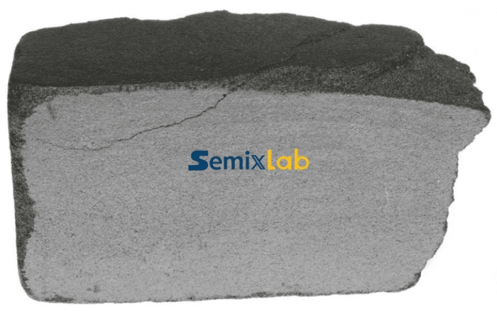
High-Purity Porous Graphite
Semixlab supplies porous graphite for applications that get hot, need things clean, and rely on gas moving through the material in a controlled way. Think semiconductor tooling, SiC crystal growth furnaces, vacuum wafer handling, and high-temperature thermal zones. We look forward to your further inquiries.
Përshkrim
Compared to a typical dense graphite grade, Semixlab supplies porous graphite breathes. It’s engineered to have a connected network of pores, which gives you predictable permeability and much better gas distribution. If your process depends on uniform temperature and steady gas flow, that’s exactly what you want.
We keep the purity tight — down around 5 ppm total impurities — so it doesn’t introduce contamination into sensitive environments. And it still has enough mechanical backbone to hold its shape through long campaigns and repeated thermal cycling.
Çfarë e bën atë ndryshe?
The pore structure is the heart of the material, and we pay a lot of attention to keeping it uniform. Gas flows the same way across the whole part, so you don’t get hot spots or dead zones that mess with process stability. That consistency pays off in higher yield and fewer unexplained drifts.
Purity is non-negotiable for semiconductor work. We start with clean raw materials and run them through advanced purification steps. The result is under 5 ppm impurities — low enough that it won’t poison your epi or crystal growth environment.
Thermally, it’s stable. Even when you’re cycling up and down between room temperature and process temperature, the dimensions barely move. That’s critical when you have tight tolerances and can’t afford parts warping or cracking mid-run.
Even with half the volume being empty space (porosity around 50%), the compressive and flexural strength hold up. You can bolt it, clamp it, stack it — it doesn’t crumble. People sometimes underestimate that, but you can machine fairly intricate shapes out of it without the edges chipping away.
And on the machining side, it’s actually quite easy to work with. We regularly cut it into blocks, plates, rings, discs, or custom forms from customer drawings. No drama.
Pse na zgjodhet ne?
✔ Purity control that meets semiconductor requirements
✔ Pore structure that’s stable batch to batch
✔ Handles thermal shock without cracking
✔ In-house machining — you don’t have to chase two vendors
✔ Prototyping and volume production both supported
✔ Deep experience in SiC and semiconductor graphite
We don’t just ship a block and wish you luck. We typically sit down with a customer’s process team, understand what they’re really trying to solve, and then tailor the pore size, grade, and machined geometry around that. It’s a lot of back and forth, but it’s the only way to get the right answer for crystal growth, epi, or advanced manufacturing.
specifikimet
Parametrat tipikë
Here’s a typical spec sheet for one of our standard porous graphite grades. Other grades and custom porosity ranges can be done — just ask.
| Vetitë fizike tipike të grafitit poroz | |
| lt | Parametër |
| dendësia Bulk | 0.89 g / cm2 |
| Forca shtypëse | 8.27 MPa |
| Forca e përkuljes | 8.27 MPa |
| Forca elastike | 1.72 MPa |
| Rezistencë specifike | 130Ω-inX10-5 |
| porosity | 50% |
| Madhësia mesatare e poreve | 70um |
| Përçueshmëri termike | 12W/M*K |
Aplikime
Where it gets used?
Rritja e kristalit të SiC – This is probably the biggest application area. You’ll find our porous graphite in SiC furnaces, where it’s used for gas distribution plates, liners, and other parts where you need gas to flow through the component itself while managing heat.
Prodhimi i gjysmëpërçuesve – Diffusion furnaces, epitaxy reactors, and other thermal processing equipment that can’t tolerate contamination. The combination of low metals and thermal stability is what matters here.
Adsorbimi me vakum – Because the pores are interconnected, you get excellent vacuum holding force across the surface. This shows up in wafer handling chucks, pick-and-place end effectors, and precision positioning systems where you need a gentle but reliable grip.
Thermal field components – Insulation rings, gas manifolds, support structures — anything that lives in a hot zone and needs to keep its shape.
Qelizat e karburantit – Some fuel cell designs rely on porous graphite for gas diffusion layers or flow-field plates. We’ve supplied material into that space as well.
FAQ
1. What pore sizes can you supply?
Standard pore sizes range from roughly 10 μm up to 100 μm. If you need something outside that window, we can usually develop a custom pore structure.
2. Can this be machined into custom shapes?
Yes. Blocks, plates, rings, discs, complex parts from your drawing — we machine them all in-house.
3. Is it clean enough for semiconductor use?
Absolutely. The high-purity grades are specifically made for contamination-sensitive environments, including semiconductor fabs and crystal growth setups.
4. Can you get the impurity levels even lower than 5 ppm?
Often yes. It depends on the application and what elements you’re trying to minimize. Additional purification steps are available if the spec demands it.
If you need high-purity porous graphite for semiconductor processing, SiC growth, or vacuum applications, reach out. We’ll talk through the specs, suggest a starting grade, and get you a quote fast.
Shërbimet tona

Dyqani i Produkteve Semixlab


